PUBLISHER: Mordor Intelligence | PRODUCT CODE: 2125643

PUBLISHER: Mordor Intelligence | PRODUCT CODE: 2125643
Japan Semiconductor Device - Market Share Analysis, Industry Trends & Statistics, Growth Forecasts (2026 - 2031)
According to Mordor Intelligence, Japan semiconductor device market size in 2026 is estimated at USD 59.29 billion, growing from 2025 value of USD 56.83 billion with 2031 projections showing USD 73.36 billion, growing at 4.34% CAGR over 2026-2031.
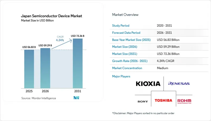
This report is Segmented by Device Type (Discrete Semiconductors, Optoelectronics, Sensors and MEMS, and Integrated Circuits), Business Model (IDM and Design/Fabless Vendor), and End-User Industry (Automotive, Communication, Consumer, Industrial, Computing/Data Storage, Data Centre, Artificial Intelligence, Government, and More). The Market Forecasts are Provided in Terms of Value (USD).
Japan Semiconductor Device Market Trends and Insights
Electric-vehicle power-train demand surge
EV architectures replace multiple mechanical parts with solid-state subsystems, elevating demand for traction inverters, on-board chargers, and ADAS controllers. Domestic leaders deploy d-mode GaN switches that outperform SiC at mid-range voltages, broadening addressable markets while retaining pricing power. Strategic partnerships between tier-one suppliers and device makers accelerate design-win cycles, ensuring that the Japan semiconductor device market benefits from higher silicon content per vehicle. Mandatory carbon-reduction targets solidify local offtake agreements, and a deep automotive ecosystem supports rapid qualification, embedding power-device gains for the medium term.
Robust 5G/6G infrastructure roll-out
Japan's mid-band densification and pre-standard 6G testbeds push throughput and latency specifications that legacy silicon cannot satisfy. Domestic RF specialists combine GaN HEMTs with proprietary matching networks to hit base-station thermal limits, cementing share while capturing premium margins. Localization of plasma-etch and MOCVD tool supply further lowers production risk, drawing additional foreign fabless orders into the Japan semiconductor device market cluster. Spillovers into network-testing equipment widen downstream opportunities, guaranteeing sustained incremental demand.
Chronic talent shortage in advanced lithography
EUV tool installations require engineers versed in sub-2 nm process integration, yet the domestic pipeline adds only a few dozen graduates per year. Multinationals lure experienced staff overseas with double-digit wage premiums, widening local gaps. Although scholarship programs and mid-career retraining provide relief, ramp schedules still hinge on expatriate hires, stretching learning curves and raising risk of yield-ramp delays that could dent the Japan semiconductor device market's near-term growth trajectory.
Other drivers and restraints analyzed in the detailed report include:
- Government subsidies for advanced-node fabs
- Consumer IoT proliferation in smart homes
- Supply-chain exposure to specialty gases and chemicals
For complete list of drivers and restraints, kindly check the Table Of Contents.
Segment Analysis
Integrated Circuits generated 85.62% of Japan semiconductor device market revenue in 2025, sustained by bespoke AI accelerators, automotive SoCs, and multilayer 3D NAND. Edge-inference ASICs consume leading-edge wafers, while high-layer NAND packages fill cloud-storage racks, anchoring volume in separate but complementary streams. Sensors and MEMS, though smaller, expand at a 5.59% CAGR as ADAS radar and factory-floor retrofits multiply attach points. Optoelectronics leverages national leadership in laser diodes for LiDAR and AR headsets. Discrete power devices grow modestly, but SiC MOSFETs and GaN transistors earn richer ASPs, stabilizing contribution margins.
A node-level view highlights a dual-track approach: sub-7 nm lines support AI and high-performance computing, whereas mature 40-65 nm flows serve car electronics and industrial control. This split lets the Japan semiconductor device market capture demand across cycles, underwriting balanced fabs that avoid over-reliance on any single customer vertical. Breakthroughs such as 1,000-layer 3D NAND will keep density leadership in the domestic ecosystem, strengthening export competitiveness.
Complete Report Scope:
- By Device Type
- Discrete Semiconductors
- Diodes
- Transistors
- Power Transistors
- Rectifier and Thyristor
- Other Discrete Semiconductors
- Optoelectronics
- Light-Emitting Diodes (LEDs)
- Laser Diodes
- Image Sensors
- Optocouplers
- Other Optoelectronics
- Sensors and MEMS
- Pressure
- Magnetic Field
- Actuators
- Acceleration and Yaw Rate
- Temperature and Other Sensors and MEMS
- Integrated Circuits
- By IC Type
- Analog
- Micro
- Microprocessors (MPU)
- Microcontrollers (MCU)
- Digital Signal Processors
- Logic
- Memory
- By Technology Node
- less than 3 nm
- 3 nm
- 5 nm
- 7 nm
- 16 nm
- 28 nm
- Above 28 nm
- By IC Type
- Discrete Semiconductors
- By Business Model
- IDM
- Design/Fabless Vendor
- By End-user Industry
- Automotive
- Communication (Wired and Wireless)
- Consumer
- Industrial
- Computing/Data Storage
- Data Centre
- Artificial Intelligence
- Government (Aerospace and Defence)
- Other End-user Industry
List of Companies Covered in this Report:
- Renesas Electronics Corporation
- Rohm Co., Ltd.
- Toshiba Electronic Devices and Storage Corporation
- Sony Semiconductor Solutions Corporation
- Kioxia Holdings Corporation
- Socionext Inc.
- Mitsubishi Electric Corporation
- Megachips Corporation
- Kyocera Corporation
- ABLIC Inc.
- Ricoh Electronic Devices Co., Ltd.
- Nisshinbo Micro Devices Inc.
- New Japan Radio Co., Ltd.
- Seiko Epson Corporation
- Seiko Instruments Inc.
- Sumitomo Electric Industries, Ltd.
- Hitachi Power Semiconductor Device, Ltd.
- Alps Alpine Co., Ltd.
- Sharp Corporation
- Fuji Electric Co., Ltd.
- Semiconductor Energy Laboratory Co., Ltd.
Additional Benefits:
- The market estimate (ME) sheet in Excel format
- 3 months of analyst support
TABLE OF CONTENTS
1 INTRODUCTION
- 1.1 Study Assumptions and Market Definition
- 1.2 Scope of the Study
2 RESEARCH METHODOLOGY
3 EXECUTIVE SUMMARY
4 MARKET LANDSCAPE
- 4.1 Market Overview
- 4.2 Market Drivers
- 4.2.1 Electric-Vehicle (EV) Power-Train Demand Surge
- 4.2.2 Robust 5G/6G Infrastructure Roll-Out
- 4.2.3 Government Subsidies for Advanced-Node Fabs
- 4.2.4 Consumer IoT Proliferation in Smart Homes
- 4.2.5 Vertical GaN/SiC RandD Leadership in Japan
- 4.2.6 Reshoring Incentives for Secure Supply Chains
- 4.3 Market Restraints
- 4.3.1 Chronic Talent Shortage in Advanced Lithography
- 4.3.2 Supply-Chain Exposure to Specialty Gases and Chemicals
- 4.3.3 Earthquake-Induced Downtime Risk for Fabs
- 4.3.4 Legacy Equipment Obsolescence for Sub-28 Nm Nodes
- 4.4 Industry Value Chain Analysis
- 4.5 Regulatory Landscape
- 4.6 Technological Outlook
- 4.7 Porter's Five Forces Analysis
- 4.7.1 Bargaining Power of Suppliers
- 4.7.2 Bargaining Power of Buyers
- 4.7.3 Threat of New Entrants
- 4.7.4 Threat of Substitutes
- 4.7.5 Intensity of Competitive Rivalry
- 4.8 Impact of Macroeconomic Factors on the Market
5 MARKET SIZE AND GROWTH FORECASTS (VALUE)
- 5.1 By Device Type
- 5.1.1 Discrete Semiconductors
- 5.1.1.1 Diodes
- 5.1.1.2 Transistors
- 5.1.1.3 Power Transistors
- 5.1.1.4 Rectifier and Thyristor
- 5.1.1.5 Other Discrete Semiconductors
- 5.1.2 Optoelectronics
- 5.1.2.1 Light-Emitting Diodes (LEDs)
- 5.1.2.2 Laser Diodes
- 5.1.2.3 Image Sensors
- 5.1.2.4 Optocouplers
- 5.1.2.5 Other Optoelectronics
- 5.1.3 Sensors and MEMS
- 5.1.3.1 Pressure
- 5.1.3.2 Magnetic Field
- 5.1.3.3 Actuators
- 5.1.3.4 Acceleration and Yaw Rate
- 5.1.3.5 Temperature and Other Sensors and MEMS
- 5.1.4 Integrated Circuits
- 5.1.4.1 By IC Type
- 5.1.4.1.1 Analog
- 5.1.4.1.2 Micro
- 5.1.4.1.2.1 Microprocessors (MPU)
- 5.1.4.1.2.2 Microcontrollers (MCU)
- 5.1.4.1.2.3 Digital Signal Processors
- 5.1.4.1.3 Logic
- 5.1.4.1.4 Memory
- 5.1.4.2 By Technology Node
- 5.1.4.2.1 less than 3 nm
- 5.1.4.2.2 3 nm
- 5.1.4.2.3 5 nm
- 5.1.4.2.4 7 nm
- 5.1.4.2.5 16 nm
- 5.1.4.2.6 28 nm
- 5.1.4.2.7 Above 28 nm
- 5.1.4.1 By IC Type
- 5.1.1 Discrete Semiconductors
- 5.2 By Business Model
- 5.2.1 IDM
- 5.2.2 Design/Fabless Vendor
- 5.3 By End-user Industry
- 5.3.1 Automotive
- 5.3.2 Communication (Wired and Wireless)
- 5.3.3 Consumer
- 5.3.4 Industrial
- 5.3.5 Computing/Data Storage
- 5.3.6 Data Centre
- 5.3.7 Artificial Intelligence
- 5.3.8 Government (Aerospace and Defence)
- 5.3.9 Other End-user Industry
6 COMPETITIVE LANDSCAPE
- 6.1 Market Concentration
- 6.2 Strategic Moves
- 6.3 Market Share Analysis
- 6.4 Company Profiles (includes Global level Overview, Market level overview, Core Segments, Financials as available, Strategic Information, Market Rank/Share for key companies, Products and Services, and Recent Developments)
- 6.4.1 Renesas Electronics Corporation
- 6.4.2 Rohm Co., Ltd.
- 6.4.3 Toshiba Electronic Devices and Storage Corporation
- 6.4.4 Sony Semiconductor Solutions Corporation
- 6.4.5 Kioxia Holdings Corporation
- 6.4.6 Socionext Inc.
- 6.4.7 Mitsubishi Electric Corporation
- 6.4.8 Megachips Corporation
- 6.4.9 Kyocera Corporation
- 6.4.10 ABLIC Inc.
- 6.4.11 Ricoh Electronic Devices Co., Ltd.
- 6.4.12 Nisshinbo Micro Devices Inc.
- 6.4.13 New Japan Radio Co., Ltd.
- 6.4.14 Seiko Epson Corporation
- 6.4.15 Seiko Instruments Inc.
- 6.4.16 Sumitomo Electric Industries, Ltd.
- 6.4.17 Hitachi Power Semiconductor Device, Ltd.
- 6.4.18 Alps Alpine Co., Ltd.
- 6.4.19 Sharp Corporation
- 6.4.20 Fuji Electric Co., Ltd.
- 6.4.21 Semiconductor Energy Laboratory Co., Ltd.
7 MARKET OPPORTUNITIES AND FUTURE OUTLOOK
- 7.1 White-space and Unmet-Need Assessment

