
PUBLISHER: Mordor Intelligence | PRODUCT CODE: 2043995

PUBLISHER: Mordor Intelligence | PRODUCT CODE: 2043995
Europe Semiconductor Silicon Wafer - Market Share Analysis, Industry Trends & Statistics, Growth Forecasts (2026 - 2031)
The Europe semiconductor silicon wafer market size in terms of shipment volume is projected to expand from 0.95 Billion Square Inches in 2025 and 0.98 Billion Square Inches in 2026 to 1.21 Billion Square Inches by 2031, registering a CAGR of 4.19% between 2026 to 2031.
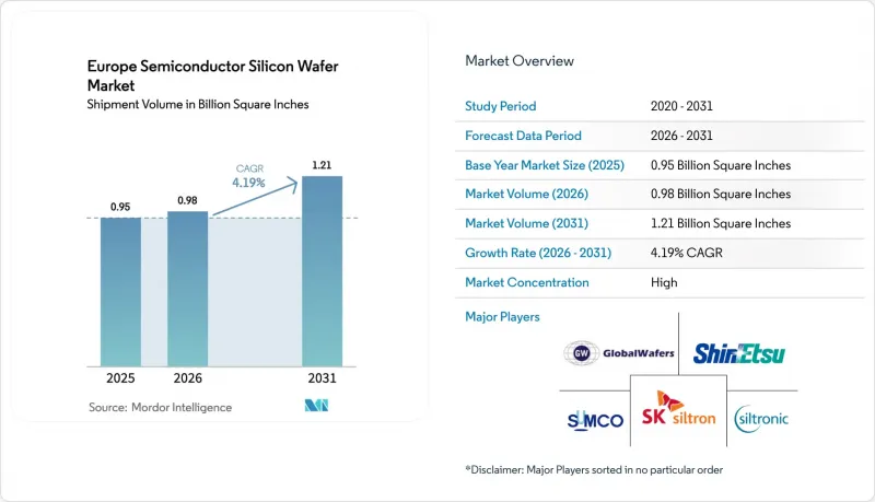
Foundry expansions backed by EU Chips Act incentives are reshaping regional supply, yet Asia continues to dominate commodity substrates, leaving room for European suppliers focused on higher-value-add niches. Automotive electrification and edge-AI adoption are tilting demand toward 300-mm prime-polished and silicon-on-insulator wafers. Power-device migration to 200 mm silicon carbide formats is sustaining a parallel-diameter stream that widens the supplier's addressable volume without cannibalizing 300 mm growth. Competitive dynamics favor incumbents with capital depth, but specialty players that master engineered substrates are capturing design wins vital to 5G, 6G, and quantum computing roadmaps.
Europe Semiconductor Silicon Wafer Market Trends and Insights
Proliferation of 300 mm Wafer Capacity in European Foundries
New 300 mm greenfield plants are reshaping cost curves for the Europe semiconductor silicon wafer market. GlobalWafers brought Italy's first 300 mm site online in October 2025, with a nameplate output of 1 million wafers per year, of which more than 60% is secured under long-term contracts with STMicroelectronics and Infineon. The European Semiconductor Manufacturing Company joint venture in Dresden will draw an extra 40,000 wafers each month when pilot runs start in late 2027, anchoring regional substrate pull for automotive nodes. Siltronic's Singapore ramp, completed in 2024, also allocates part of its 300 mm output to European buyers facing capacity rationing. Together, these projects lift regional bargaining power on polysilicon pricing and shorten logistics loops for critical automotive and industrial volumes.
Growing Demand for Power Electronics in EV and Renewable Grid
Electrification targets are steering wafer mix toward high-voltage devices fabricated on both silicon and silicon carbide. Infineon began 200 mm SiC processing in Villach during the first quarter of 2025, enabling traction inverters that must handle voltages above 1,200 V. STMicroelectronics mirrored that move at Catania in the fourth quarter, and onsemi committed up to USD 2 billion for end-to-end SiC capacity in the Czech Republic. EU-backed Transform and related programs are knitting together a European SiC value chain that reduces reliance on Asian ingot suppliers. Demand also comes from grid-scale solar inverters and wind turbines that use ruggedized power modules, thereby driving broader substrate uptake.
Limited Polysilicon Feedstock Supply within Europe
Wacker Chemie's July 2025 etching-line expansion lifted regional semiconductor-grade polysilicon output by more than 50% but Europe still imports over 70% of feedstock from Asia. Heavy reliance on external sources exposes wafer makers to geopolitical shocks and price spikes. Building an integrated silicon carbide supply under the Transform program shows the scale of capital and environmental permitting hurdles that constrain upstream diversification. Until additional purification capacity comes online or binding long-term offtake deals are signed, feedstock tightness will cap upside for European wafer shipments.
Other drivers and restraints analyzed in the detailed report include:
- EU Chips Act Incentives for Domestic Semiconductor Manufacturing
- Adoption of Silicon-On-Insulator Wafers for RF and 5G Front-End Modules
- High Capital Intensity and Long ROI Deterring New Entrants
For complete list of drivers and restraints, kindly check the Table Of Contents.
Segment Analysis
The 300 mm node delivered 73.61% of shipments in 2025, confirming its position as the workhorse format for logic and memory processes that dominate European fab roadmaps. GlobalWafers' Novara launch and the forthcoming ESMC Dresden ramp collectively add more than 1.5 million wafers to the annual 300 mm capacity, deepening the Europe semiconductor silicon wafer market for prime-polished substrates. Cost-per-die advantages, compatibility with EUV lithography, and tight coupling to automotive-qualified process flows keep 300 mm utilisation high.
Parallel demand for 200 mm persists, propelled by silicon carbide power devices and analog products tailored to automotive electrification. Infineon's Villach and STMicroelectronics' Catania conversions prove that crystal-growth realities and defect budgets still favor 200 mm for SiC wafers. Consequently, the Europe semiconductor silicon wafer market retains a dual-diameter structure where 300 mm drives volume and 200 mm secures margin resilience, while up to 150 mm lines remain focused on MEMS and optoelectronic niches served by Okmetic's sensor-grade output.
Logic wafers represented 32.74% of 2025 volume, benefiting from edge-AI accelerators and automotive microcontrollers that rely on 28 nm-65 nm nodes, processes that European fabs are adding at scale. The Dresden joint venture between TSMC, Bosch, Infineon, and NXP focuses on precisely those geometries, which should widen the Europe semiconductor silicon wafer market size allocated to logic over the forecast horizon.
Memory holds a smaller slice due to Europe's limited commodity DRAM output, yet embedded non-volatile memory tied to FD-SOI projects keeps niche growth alive. Analog and mixed-signal devices ride industrial automation and sensor interface demand, while silicon carbide discretes for high-voltage drives are the fastest climber in the Europe semiconductor silicon wafer market, spurring a wave of epitaxial wafer orders from power-device manufacturers.
The Europe Semiconductor Silicon Wafer Market Report is Segmented by Wafer Diameter (Up To 150 Mm, 200 Mm, 300 Mm), Semiconductor Device Type (Logic, Memory, Analog, Discrete, Optoelectronics, Sensors, Micro), Wafer Type (Prime Polished, Epitaxial, Silicon-On-Insulator, Specialty Silicon), End-User (Telecommunications, and More), and Country. The Market Forecasts are Provided in Terms of Shipments by Volume (Square Inches).
List of Companies Covered in this Report:
- Shin-Etsu Chemical Co., Ltd.
- SUMCO Corporation
- GlobalWafers Co., Ltd.
- Siltronic AG
- SK siltron Co., Ltd.
- SOITEC S.A.
- Okmetic Oy
- Wafer Works Corporation
- LG Siltron
- Shanghai Simgui Technology Co., Ltd.
- Topsil Semiconductor Materials A/S
- MEMC Electronic Materials, Inc. (GlobalFoundries)
- LOGOS Wafer Manufacturing
- Air Liquide Electronics
- NSIG Group
- Advanced Silicon S.A.
- Sumitomo Mitsubishi Silicon Corporation (SMS)
Additional Benefits:
- The market estimate (ME) sheet in Excel format
- 3 months of analyst support
TABLE OF CONTENTS
1 INTRODUCTION
- 1.1 Study Assumptions and Market Definition
- 1.2 Scope of the Study
2 RESEARCH METHODOLOGY
3 EXECUTIVE SUMMARY
4 MARKET LANDSCAPE
- 4.1 Market Overview
- 4.2 Industry Value-Chain Analysis
- 4.3 Market Drivers
- 4.3.1 Proliferation of 300 mm Wafer Capacity in European Foundries
- 4.3.2 Growing Demand for Power Electronics in EV and Renewable Grid
- 4.3.3 EU Chips Act Incentives for Domestic Semiconductor Manufacturing
- 4.3.4 Adoption of Silicon-on-Insulator Wafers for RF and 5G Front-End Modules
- 4.3.5 Edge AI Adoption Driving 200 mm Logic and Analog Node Revivals
- 4.3.6 Emerging High-Resistivity Wafers for Quantum Computing R&D
- 4.4 Market Restraints
- 4.4.1 Limited Polysilicon Feedstock Supply within Europe
- 4.4.2 High Capital Intensity and Long ROI Deterring New Entrants
- 4.4.3 Geopolitical Dependency on Asia for Wafer Processing Equipment
- 4.4.4 Environmental Regulations Increasing Cost of Ultrapure Water Usage
- 4.5 Regulatory Landscape
- 4.6 Technological Outlook
- 4.7 Impact of Macroeconomic Factors
- 4.8 Porter's Five Forces Analysis
- 4.8.1 Bargaining Power of Suppliers
- 4.8.2 Bargaining Power of Buyers
- 4.8.3 Threat of New Entrants
- 4.8.4 Threat of Substitutes
- 4.8.5 Intensity of Competitive Rivalry
5 MARKET SIZE AND GROWTH FORECASTS (SHIPMENT IN AREA)
- 5.1 By Wafer Diameter
- 5.1.1 Up to 150 mm
- 5.1.2 200 mm
- 5.1.3 300 mm
- 5.2 By Semiconductor Device Type
- 5.2.1 Logic
- 5.2.2 Memory
- 5.2.3 Analog
- 5.2.4 Discrete
- 5.2.5 Optoelectronics
- 5.2.6 Sensors
- 5.2.7 Micro (MCU, MPU, DSP)
- 5.3 By Wafer Type
- 5.3.1 Prime Polished
- 5.3.2 Epitaxial
- 5.3.3 Silicon-on-Insulator (SOI)
- 5.3.4 Specialty Silicon (High-Resistivity, Power, Sensor-Grade)
- 5.4 By End-User
- 5.4.1 Consumer Electronics
- 5.4.1.1 Mobile and Smartphones
- 5.4.1.2 PCs and Servers
- 5.4.2 Industrial
- 5.4.3 Telecommunications
- 5.4.4 Automotive
- 5.4.5 Other End-User Applications
- 5.4.1 Consumer Electronics
- 5.5 By Country
- 5.5.1 Germany
- 5.5.2 France
- 5.5.3 United Kingdom
- 5.5.4 Italy
- 5.5.5 Spain
- 5.5.6 Russia
- 5.5.7 Rest of Europe
6 COMPETITIVE LANDSCAPE
- 6.1 Market Concentration
- 6.2 Strategic Moves
- 6.3 Market Share Analysis
- 6.4 Company Profiles (includes Global Level Overview, Market Level Overview, Core Segments, Financials as available, Strategic Information, Market Rank/Share, Products and Services, Recent Developments)
- 6.4.1 Shin-Etsu Chemical Co., Ltd.
- 6.4.2 SUMCO Corporation
- 6.4.3 GlobalWafers Co., Ltd.
- 6.4.4 Siltronic AG
- 6.4.5 SK siltron Co., Ltd.
- 6.4.6 SOITEC S.A.
- 6.4.7 Okmetic Oy
- 6.4.8 Wafer Works Corporation
- 6.4.9 LG Siltron
- 6.4.10 Shanghai Simgui Technology Co., Ltd.
- 6.4.11 Topsil Semiconductor Materials A/S
- 6.4.12 MEMC Electronic Materials, Inc. (GlobalFoundries)
- 6.4.13 LOGOS Wafer Manufacturing
- 6.4.14 Air Liquide Electronics
- 6.4.15 NSIG Group
- 6.4.16 Advanced Silicon S.A.
- 6.4.17 Sumitomo Mitsubishi Silicon Corporation (SMS)
7 MARKET OPPORTUNITIES AND FUTURE OUTLOOK
- 7.1 White-Space and Unmet-Need Assessment

