
PUBLISHER: Mordor Intelligence | PRODUCT CODE: 2043996

PUBLISHER: Mordor Intelligence | PRODUCT CODE: 2043996
Germany Semiconductor Silicon Wafer - Market Share Analysis, Industry Trends & Statistics, Growth Forecasts (2026 - 2031)
The Germany semiconductor silicon wafer market size in terms of shipment volume was valued at 263.04 Million Square Inches in 2025 and is estimated to grow from 273.85 Million Square Inches in 2026 to reach 341.35 Million Square Inches by 2031, at a CAGR of 4.51% during the forecast period (2026-2031).
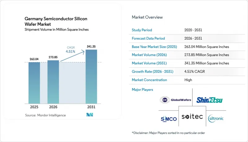
A multi-year build-out of 300 mm logic and power-device fabs, anchored by Intel, TSMC, Infineon, and GlobalFoundries, is lifting long-term demand for prime polished and epitaxial substrates while tightening contract pricing. Corporate power-purchase agreements for wind and solar electricity are beginning to close the historical energy-cost gap with Asia, strengthening the competitiveness of Germany's semiconductor silicon wafer market. Parallel shifts toward float-zone high-purity wafers for quantum initiatives and fully depleted SOI for automotive radar add specialty upside. At the same time, volatile polysilicon pricing and elevated industrial tariffs keep near-term margins under pressure, compelling producers to prioritize high-value segments and long-term offtake contracts.
Germany Semiconductor Silicon Wafer Market Trends and Insights
Strong Capex Pipeline for 300 Mm Fab Expansions in Germany
Intel broke ground on two Magdeburg fabs in mid-2025 as part of a EUR 30 billion (USD 34 billion) commitment that will deliver sub-5 nm logic capacity when production starts in 2028. TSMC, Bosch, Infineon, and NXP jointly launched the European Semiconductor Manufacturing Company in Dresden, a EUR 10 billion (USD 11.3 billion) venture slated to produce 40,000 wafers per month at 28 nm, 22 nm, and 16 nm nodes by 2027. Infineon's EUR 5 billion (USD 5.7 billion) Smart Power Fab, which entered pilot output in early 2025, targets silicon carbide and high-voltage silicon on 300 mm lines. GlobalFoundries is adding more than 1 million 300 mm wafers per year to its Dresden plant through a EUR 1.1 billion (USD 1.25 billion) expansion that was completed in 2028. Collectively, these projects compress polished-wafer lead times and secure multi-year offtake agreements that underpin the market's long-term growth trajectory.
Revival of Automotive Chip Demand Post-2025
German vehicle output rebounded to 4.1 million units in 2024, restoring chip orders that had stalled during the 2022-2023 inventory correction. Infineon reported double-digit growth in power-device shipments for electric-vehicle drivetrains during fiscal 2025, with silicon carbide MOSFETs delivering 3% efficiency gains over silicon IGBTs in production models such as the Porsche Taycan. Demand is reinforced by the shift to 800 V battery systems that require high-voltage epitaxial wafers with sub-2% doping variation. Euro 7 rules, effective 2025, require multiple sensors and microcontrollers per car, further increasing wafer volume requirements. As automakers lock in supply, wafer sellers benefit from longer contracts and tighter specification premiums.
Volatile Polysilicon Pricing
Semiconductor-grade polysilicon plunged from USD 35 kg-1 in early 2022 to USD 6.5 kg-1 by December 2024 after Chinese suppliers added 400,000 t of annual capacity. Siltronic said raw-material costs fell 12% in H1 2025 but warned that spot quotes remain 40% beneath long-term contract floors, clouding investment planning. A rapid rebound toward USD 20 kg-1 would slice 3-5 percentage points from wafer-maker margins unless device customers accept price increases. The unpredictability deters smaller producers from green-lighting new Czochralski pullers, effectively consolidating share with vertically integrated rivals that refine their own feedstock. Until pricing stabilizes, the supply base will stay cautious on incremental capacity.
Other drivers and restraints analyzed in the detailed report include:
- EU Chips Act Incentives for On-Shore Wafer Production
- Increasing Adoption of Power Devices for E-Mobility
- High Energy Costs Versus Asian Peers
For complete list of drivers and restraints, kindly check the Table Of Contents.
Segment Analysis
The Germany semiconductor silicon wafer market recorded 300 mm substrates at a commanding 74.68% volume share in 2025, outstripping all other diameters. Tooling for leading-edge logic and automotive power devices is standardized around this format, which delivers more than twice the usable die area of 200 mm alternatives, trimming per-chip processing cost by roughly 30%. Intel's Magdeburg fabs impose site-flatness below 0.08 µm and total-thickness variation under 0.15 µm, specifications that narrow the approved-vendor list to Shin-Etsu and SUMCO's premium grades.
Contract prices for 300 mm prime-polished wafers rose to low-to-mid single digits year over year in 2025 as crystal-puller lead times stretched to 24 months. The 200 mm tier retains strategic relevance for analog, MEMS, and discrete manufacturing; X-FAB's Erfurt line, fully dedicated to 200 mm, captures industrial sensor demand where die sizes exceed 10 mm2. Diameters of 150 mm and below are largely confined to legacy optoelectronics, and capacity is expected to consolidate further as vendors rationalize older furnaces.
Logic wafers accounted for 36.82% of 2025 shipments, reflecting Germany's transition toward edge AI controllers and integrated automotive domain processors. TSMC's Dresden plant alone will process 40,000 300 mm wafers a month at 28 nm, 22 nm, and 16 nm, cementing logic's pull on prime-polished supply. Memory's footprint remains smaller because Germany hosts limited DRAM or NAND front-end capacity, yet data-center growth is spurring tentative interest in specialty memory tie-ups.
Analog and mixed-signal devices, essential for industrial sensor arrays, consumed over one-fifth of wafer volume, aided by Industry 4.0 rollouts. Discrete and power components, including silicon carbide MOSFETs for EV drivetrains, command premium unit pricing, helping producers offset softer consumer-electronics margins. The convergence of logic and analog in fully depleted SOI platforms further blurs device-type boundaries and increases process-flow flexibility.
The Germany Semiconductor Silicon Wafer Market Report is Segmented by Wafer Diameter (Up To 150 Mm, 200 Mm, 300 Mm), Semiconductor Device Type (Logic, Memory, Analog, Discrete, and More), Wafer Type (Prime Polished, Epitaxial, Silicon-On-Insulator (SOI), Specialty Silicon), End-User (PCs and Servers, Telecommunications, Automotive, and More). The Market Forecasts are Provided in Terms of Shipments by Volume (Square Inches).
List of Companies Covered in this Report:
- Siltronic AG
- Shin-Etsu Handotai Co., Ltd.
- SUMCO Corporation
- GlobalWafers Co., Ltd.
- Soitec S.A.
- Okmetic Oy
- SK Siltron Co., Ltd.
- Wafer Works Corporation
- Topsil Semiconductor Materials A/S
- Ferrotec Holdings Corporation
- MEMC Electronic Materials, Inc.
- Zhonghuan Semiconductor Co., Ltd.
- Hebei Shangyi Electronic Materials Co., Ltd.
- Linton Crystal Technologies
- Hangzhou Silicon Tech Co., Ltd.
- Advanced Micro Foundry Pte Ltd.
- Sil'tronix Silicon Technologies
- IQE plc
- Episil-Precision Inc.
- MCL Electronic Materials Ltd.
Additional Benefits:
- The market estimate (ME) sheet in Excel format
- 3 months of analyst support
TABLE OF CONTENTS
1 INTRODUCTION
- 1.1 Study Assumptions and Market Definition
- 1.2 Scope of the Study
2 RESEARCH METHODOLOGY
3 EXECUTIVE SUMMARY
4 MARKET LANDSCAPE
- 4.1 Market Overview
- 4.2 Market Drivers
- 4.2.1 Strong CAPEX Pipeline for 300 mm Fab Expansions in Germany
- 4.2.2 Revival of Automotive Chip Demand Post-2025
- 4.2.3 EU Chips Act Incentives for On-shore Wafer Production
- 4.2.4 Increasing Adoption of Power Devices for E-Mobility
- 4.2.5 Shift Toward Float-Zone High-Purity Wafers for Quantum-Tech
- 4.2.6 Corporate PPAs Driving Renewable-Powered Wafer Plants
- 4.3 Market Restraints
- 4.3.1 Volatile Polysilicon Pricing
- 4.3.2 High Energy Costs Versus Asian Peers
- 4.3.3 Talent Shortage in Crystal-Growing Specialists
- 4.3.4 Tightening ESG Audits on Scope-3 Emissions
- 4.4 Industry Value-Chain Analysis
- 4.5 Technology Analysis
- 4.6 Regulatory Landscape
- 4.7 Impact of Macroeconomic Factors
- 4.8 Porter's Five Forces Analysis
- 4.8.1 Bargaining Power of Suppliers
- 4.8.2 Bargaining Power of Buyers
- 4.8.3 Threat of New Entrants
- 4.8.4 Threat of Substitutes
- 4.8.5 Intensity of Competitive Rivalry
5 MARKET SIZE AND GROWTH FORECASTS (VOLUME)
- 5.1 By Wafer Diameter
- 5.1.1 Up to 150 mm
- 5.1.2 200 mm
- 5.1.3 300 mm
- 5.2 By Semiconductor Device Type
- 5.2.1 Logic
- 5.2.2 Memory
- 5.2.3 Analog
- 5.2.4 Discrete
- 5.2.5 Other Semiconductor Device Types (Optoelectronics, Sensors, Micro)
- 5.3 By Wafer Type
- 5.3.1 Prime Polished
- 5.3.2 Epitaxial
- 5.3.3 Silicon-on-Insulator (SOI)
- 5.3.4 Specialty Silicon (High-Resistivity, Power, Sensor-Grade)
- 5.4 By End-user
- 5.4.1 Consumer Electronics
- 5.4.2 Mobile and Smartphones
- 5.4.3 PCs and Servers
- 5.4.4 Industrial
- 5.4.5 Telecommunications
- 5.4.6 Automotive
- 5.4.7 Other End-user Applications
6 COMPETITIVE LANDSCAPE
- 6.1 Market Concentration
- 6.2 Strategic Moves (M&A, Capacity, JV)
- 6.3 Market Share Analysis
- 6.4 Company Profiles (includes Global Level Overview, Market Level Overview, Core Segments, Financials as available, Strategic Information, Market Rank/Share, Products and Services, Recent Developments)
- 6.4.1 Siltronic AG
- 6.4.2 Shin-Etsu Handotai Co., Ltd.
- 6.4.3 SUMCO Corporation
- 6.4.4 GlobalWafers Co., Ltd.
- 6.4.5 Soitec S.A.
- 6.4.6 Okmetic Oy
- 6.4.7 SK Siltron Co., Ltd.
- 6.4.8 Wafer Works Corporation
- 6.4.9 Topsil Semiconductor Materials A/S
- 6.4.10 Ferrotec Holdings Corporation
- 6.4.11 MEMC Electronic Materials, Inc.
- 6.4.12 Zhonghuan Semiconductor Co., Ltd.
- 6.4.13 Hebei Shangyi Electronic Materials Co., Ltd.
- 6.4.14 Linton Crystal Technologies
- 6.4.15 Hangzhou Silicon Tech Co., Ltd.
- 6.4.16 Advanced Micro Foundry Pte Ltd.
- 6.4.17 Sil'tronix Silicon Technologies
- 6.4.18 IQE plc
- 6.4.19 Episil-Precision Inc.
- 6.4.20 MCL Electronic Materials Ltd.
7 MARKET OPPORTUNITIES AND FUTURE OUTLOOK
- 7.1 White-space And Unmet-Need Assessment

